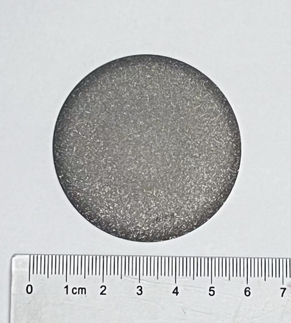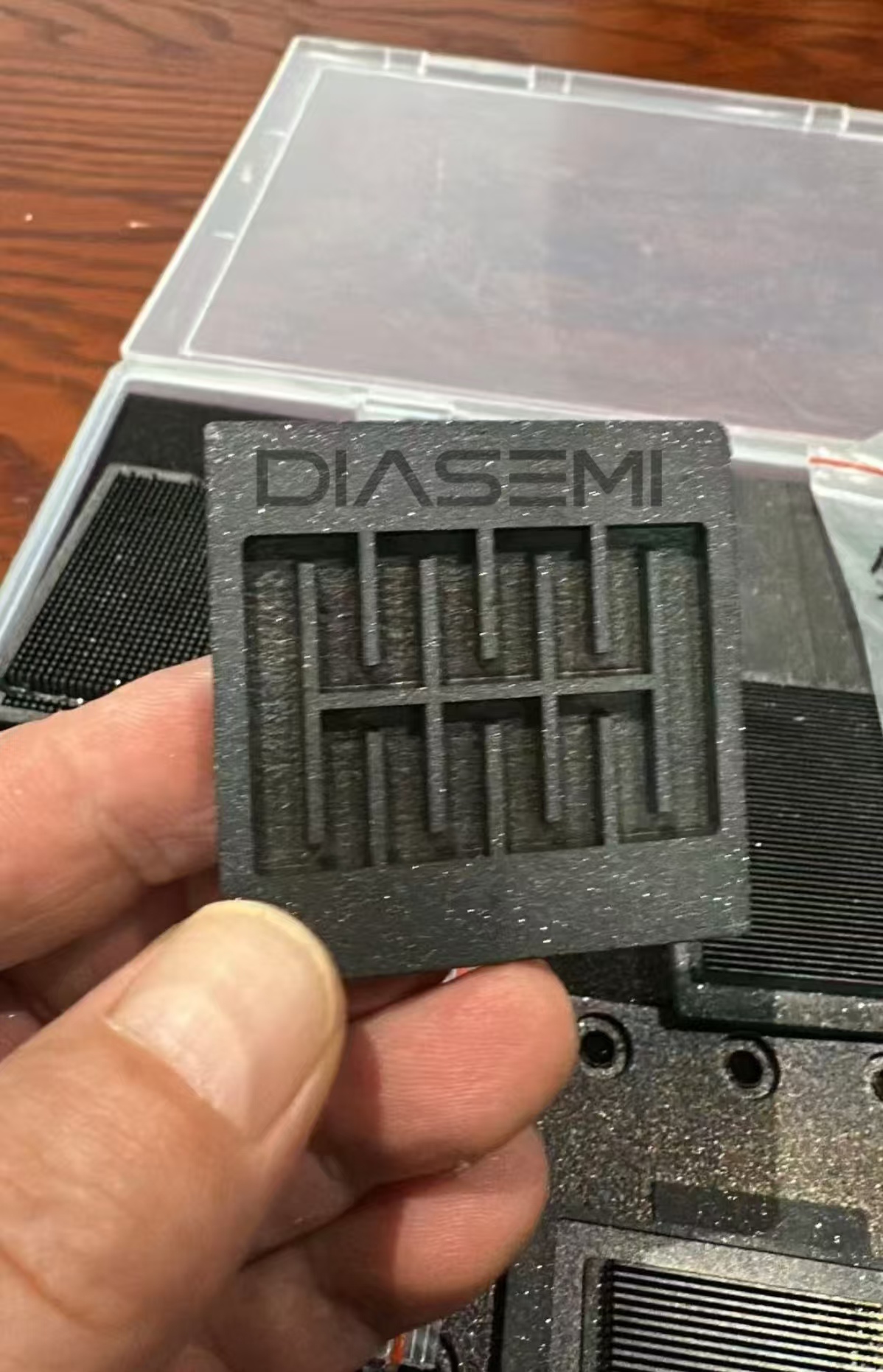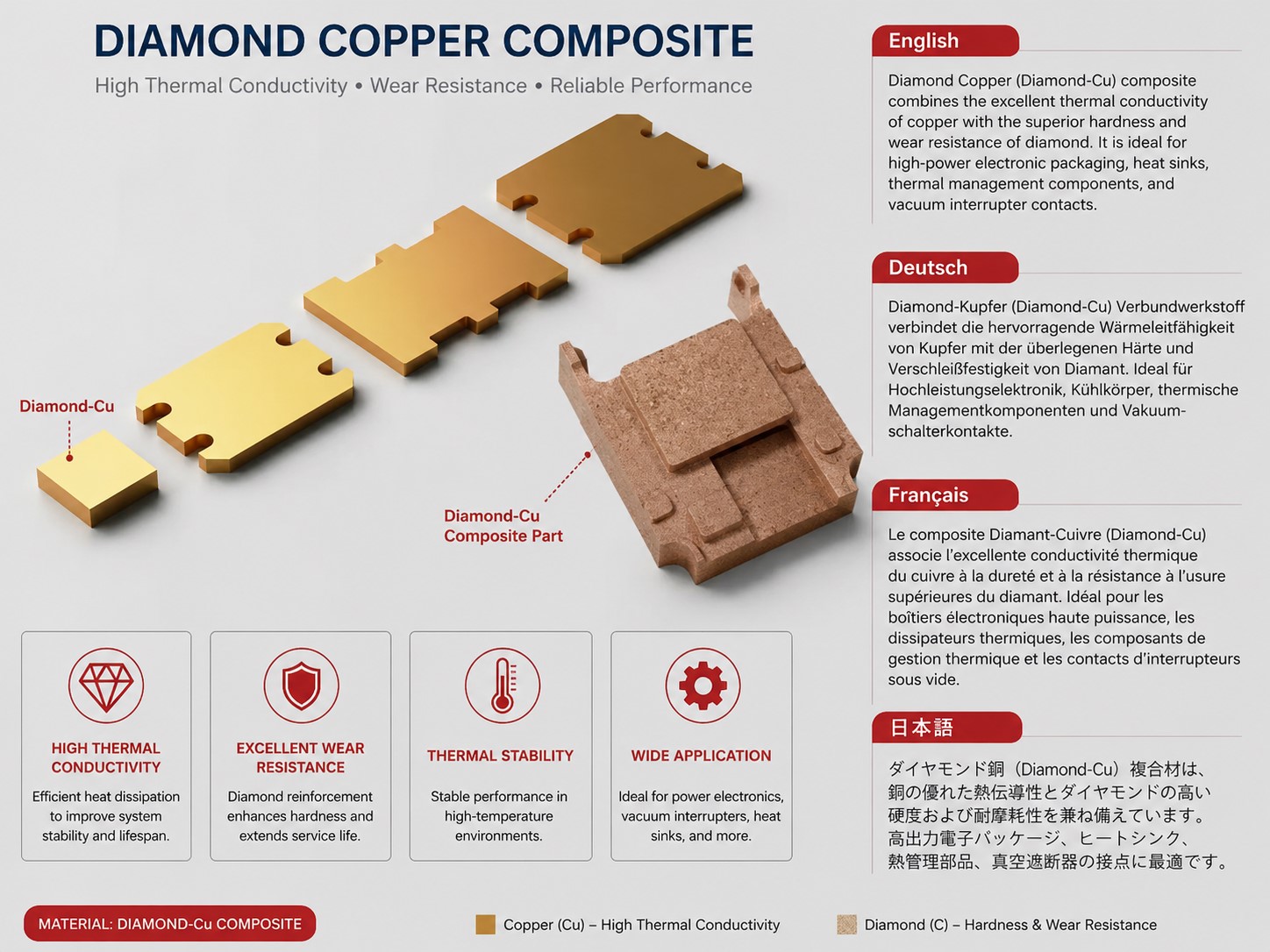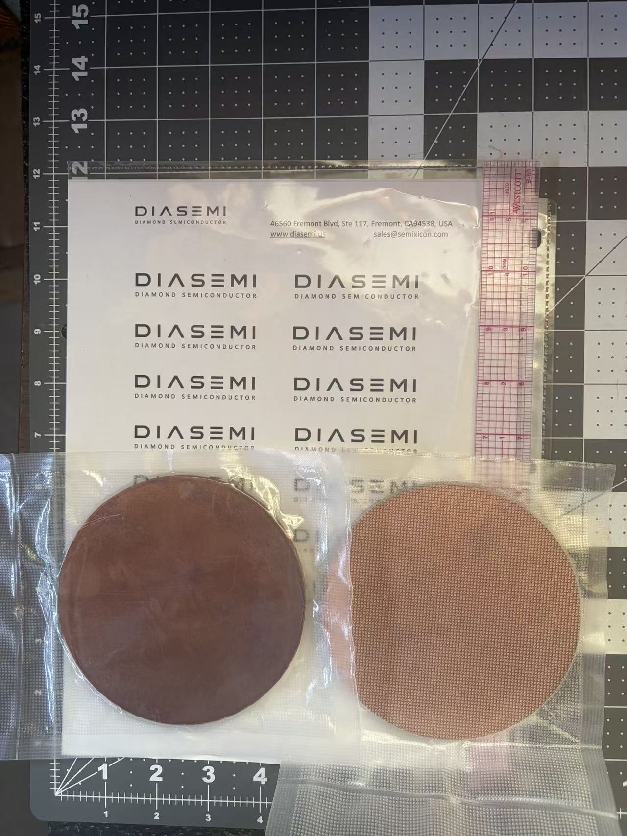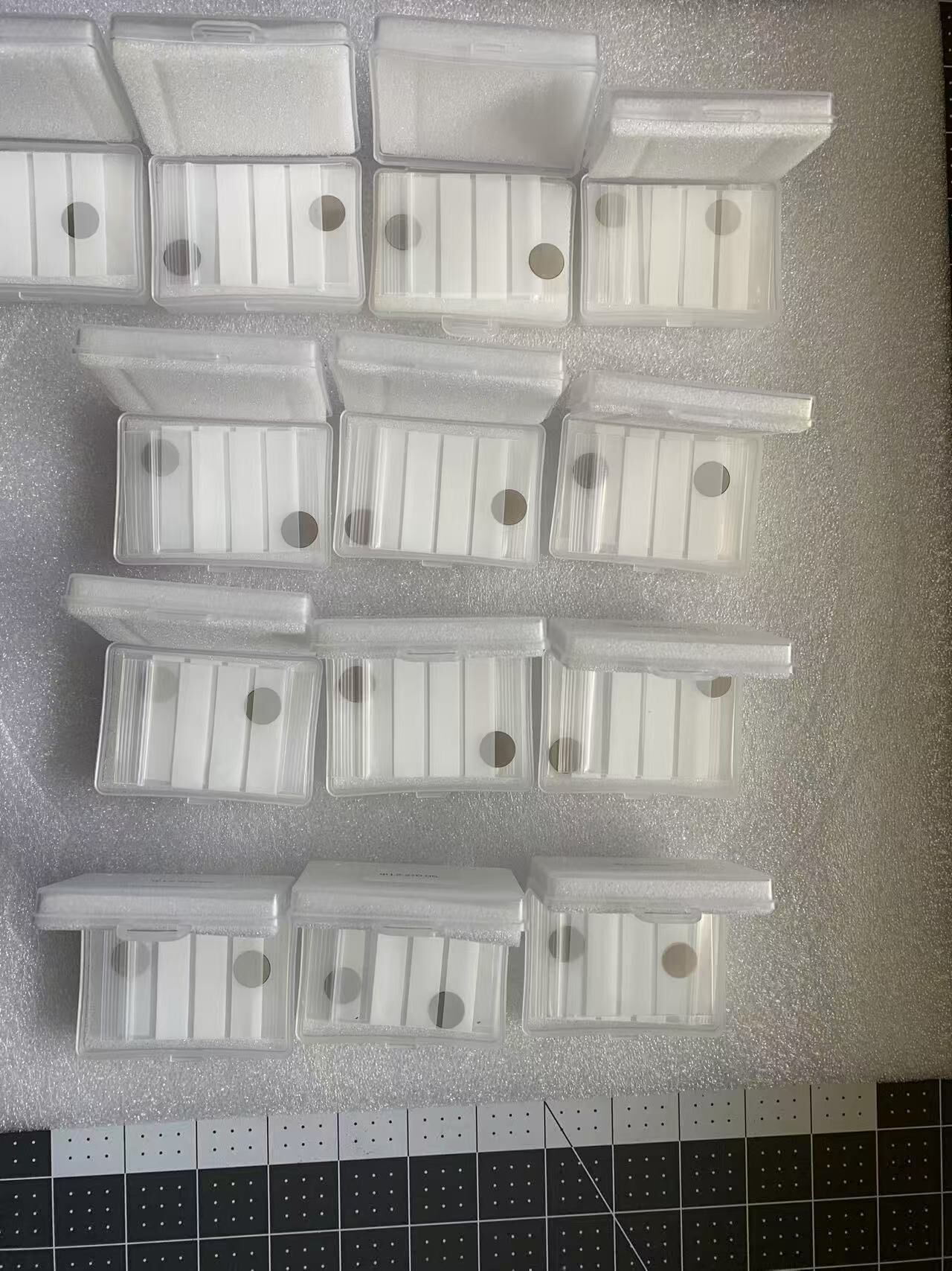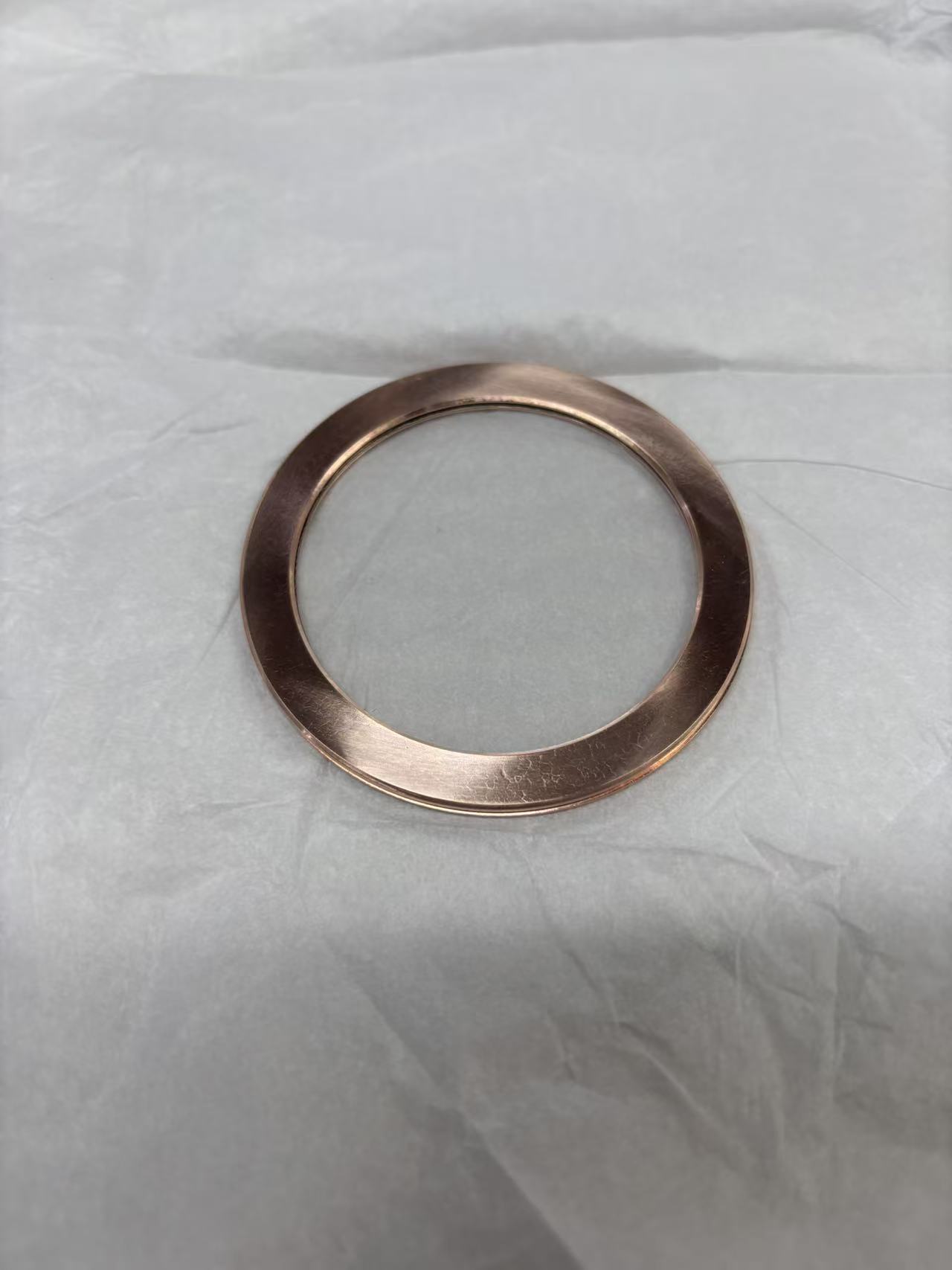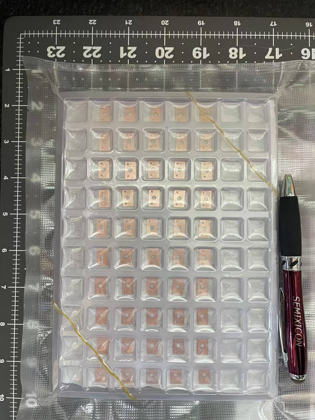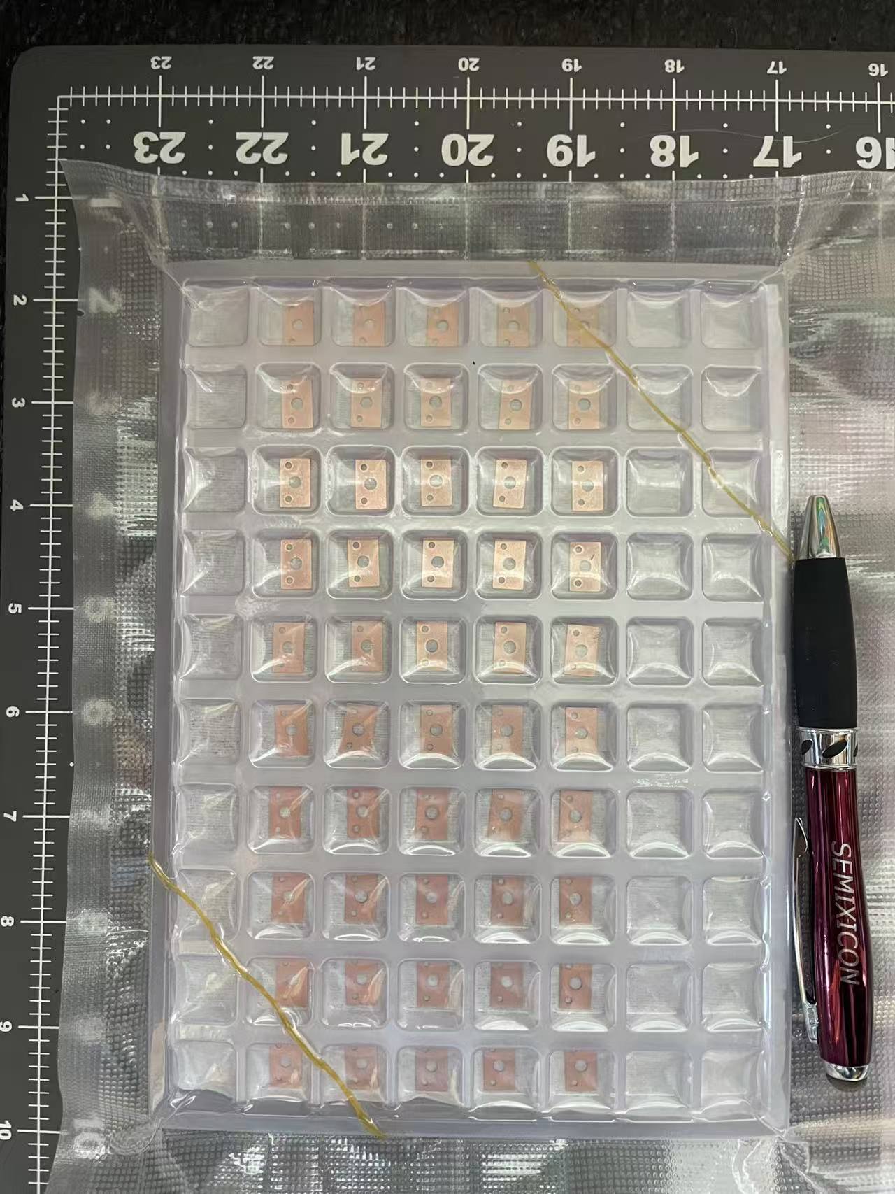
DIASEMI Diamond Double-Sided Thick-Copper TDV Substrate
Ultra-High Thermal Conductivity. High-Current Capability. True 3D Interconnection.
The rapid growth of AI computing, low-altitude systems, optical communications, 6G, RF, power electronics, lasers and advanced photonics is driving semiconductor devices toward unprecedented power density, operating frequency and integration. As localized heat flux approaches and exceeds 300 W/cm², conventional AlN and Al₂O₃ ceramic substrates increasingly face limitations in thermal dissipation, current carrying capacity and high-frequency interconnection. Conventional single-sided diamond substrates, meanwhile, remain primarily planar and cannot fully support three-dimensional circuit integration.
DIASEMI introduces a new generation of diamond-based double-sided thick-copper substrates with Through-Diamond Via (TDV) technology, combining ultra-high thermal conductivity, high-current power distribution and vertical electrical interconnection within a single substrate architecture.
A New Thermal-Electrical Substrate Architecture
Built on high-thermal-conductivity CVD diamond, the DIASEMI platform integrates precision diamond processing, low-stress interface engineering, double-sided thick-copper metallization and high-aspect-ratio TDV technology.
Copper circuitry with thicknesses of ≥50 μm can be formed on both surfaces of the diamond substrate, while metallized through-diamond vias establish direct vertical connections between the upper and lower circuits.
This architecture transforms the substrate from a conventional planar carrier into a three-dimensional thermal-electrical platform. Diamond provides a continuous, electrically insulating thermal path, while thick copper provides low-resistance power and signal routing. The result is a compact structure capable of simultaneously supporting heat spreading, high-current transmission and vertical interconnection.
Key Performance Advantages
>1,300 W/m·K Thermal Conductivity The high thermal conductivity of diamond rapidly spreads localized heat from active devices, helping reduce thermal gradients and junction temperatures. This makes the platform particularly attractive for high-power and high-heat-flux electronics.
≥50 μm Double-Sided Copper Thick copper provides substantially greater current-carrying capability than conventional thin-film metallization while enabling independent routing of power, control and RF circuits on both surfaces.
Through-Diamond Via (TDV) Metallized diamond vias create short, low-resistance vertical interconnection paths between both sides of the substrate. TDV enables three-dimensional circuit integration while reducing routing distance and interconnection complexity.
Thermal–Electrical Co-Design Unlike conventional multilayer ceramic structures, the DIASEMI architecture integrates heat spreading and electrical interconnection directly into the diamond substrate, providing a highly compact platform for high-power and high-frequency devices.
Enabling Next-Generation Electronics
DIASEMI Diamond Double-Sided Thick-Copper TDV Substrates are designed for demanding applications including:
2–18 GHz broadband RF devices and T/R modules
6G millimeter-wave front-end systems
High-power RF amplifiers
Laser, photonic and high-power LED modules
Power electronics and high-density power modules
AI computing and advanced semiconductor packaging
Chiplet and heterogeneous integration
The platform can also be integrated with silicon IPD, HTCC and other advanced packaging technologies, providing a high-thermal-flux carrier for multi-die and heterogeneous systems.
From Diamond Material to 3D Packaging
DIASEMI integrates CVD diamond growth, precision grinding and polishing, thick-copper patterning, via formation and TDV metallization into an advanced diamond substrate technology platform.
By combining the world's highest-performance thermal material with high-current copper circuitry and vertical interconnection, DIASEMI is moving semiconductor substrates beyond conventional planar architectures toward 3D thermal-electrical integration.
DIASEMI Diamond Materials & Advanced Packaging Technologies Enabling the next generation of high-power, high-frequency and high-density electronics.
BJT: bipolar junction transistor
FET: field effect transistor
SAW: sound acoustic wave
MPA: microwaver power amplificator
TWT: traveling wave tube